What's new

BCM4916 process node?

  • SNBForums Code of Conduct

    SNBForums is a community for everyone, no matter what their level of experience.

    Please be tolerant and patient of others, especially newcomers. We are all here to share and learn!

    The rules are simple: Be patient, be nice, be helpful or be gone!

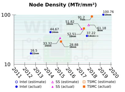
14nm Samsung and 16nm TSMC are a similar density. QCA HW has been on 14nm Samsung FinFET for a bit now (2018+)

Broadcom sticks to cheaper nodes because they value pricing/yield, etc. I would assume TSMC finally offered them a deal to move up to 16nm.

TSMC was trying to free up 28nm capacity a couple years ago. IE: https://www.anandtech.com/show/17470/tsmc-to-customers-time-to-stop-using-older-nodes-move-to-28nm


I wouldn't expect any smaller unless the price/yield makes sense for both companies.
 
Last edited:
I have RT-AX88U Pro (BCM4912) with the stock firmware.
It seems to be running pretty cool.
`/sys/devices/virtual/thermal/thermal_zone0/temp` says 55C (ambient is 20C).

The stock firmware has the `stress` utility build-in. I tried to run for 5 minutes with 8 threads to load the cpu (`stress cpu -e 8 -t 600`) and I only got to 62C.

It would be nice if there was a way to see at which frequency is running under stress. Specifically if's holding 2 GHz on all cores.
I tried to look in /sys and do some googling but I can't find any cpufreq reporting.
Is there a reason for using -e 8 instead of -e 4? Those CPUs are only Quad cores without hyperthreading.

Also I saw someone used
Code:
./stress-ng --cpu 4 -t 300
to stress test their ASUS router with stock firmware in a video, not sure how he did it, I can't get stress-ng working on mine.
 
Hi, I read that the BCM4908 is made using the 28nm process, and the B4912 is made using TSMC’s 16nm process, but I can’t find any information about the BCM4916 regarding process node online. Does anyone know which process it use?

I don't think there is anyone really qualified to say which process node is better and why a die-shrink could be beneficial...

These are comms processors that work with a specific set of requirements - they're not general purpose application processors.

Let the design engineers work the balance between cost and performance to meet the targeted goals...
 
I don't think there is anyone really qualified to say which process node is better and why a die-shrink could be beneficial...
What? So there are pros of using a 16nm process over 7nm, other than cost?

You know that Filogic 880 from MKT uses 6nm quad-core A73, Networking Pro 1220 from Qualcomm uses 14nm quad-core A73, while BCM4916 is still on quad-core A53 (or B53 if you prefer), with a likely 16nm process, which is significantly lagging behind, right?

 
It depends on design constraints for company.

Broadcom reused AC W2 28nm CPUs up until the 2nd gen AX revision, where QCA went full in on Samsung 14nm FinFET in 2018 with the introduction of AX.

It's not rocket science why certain brands stick to specific nodes.
 

Attachments

  • tsmc-density-with-7nm (1).jpeg
    tsmc-density-with-7nm (1).jpeg
    185 KB · Views: 38
Last edited:
What? So there are pros of using a 16nm process over 7nm, other than cost?

You know that Filogic 880 from MKT uses 6nm quad-core A73, Networking Pro 1220 from Qualcomm uses 14nm quad-core A73, while BCM4916 is still on quad-core A53 (or B53 if you prefer), with a likely 16nm process, which is significantly lagging behind, right?


Again, I think mostly it'll be down to cost - something like 7nm is going to be more expensive than a 12/14nm node, and those will be more than 22nm where we first saw FinFet, and 28nm planar...

Consider that if the major elements, in this case, the switch in the SoC - if it's still at 28nm, then why do a shrink down?

The fabless vendors like Qualcomm, Broadcom, Mediatek - they have to license the tools and the utility libraries from companies like Synopsys and Cadence, and that even before buying into a node process from TSMC, SMIC, GloFo, Samsung, etc... and all the fabs have their own design rules about which tools to use, and how to integrate into their process...

There's a lot of data points to consider when making a decision to commit to a fab and which node to use...
 
Fabless companies are also subject to set order wafer cost.

It's sometimes more logical to go smaller if the yield is high. Depends on the overall logistics and design constraint.

NVIDIA went 8nm Samsung for Ampere because TSMC wouldn't really budge on 7nm. 8nm SS is a crappy node, but it made sense given the kickbacks.
 
What? So there are pros of using a 16nm process over 7nm, other than cost?

You know that Filogic 880 from MKT uses 6nm quad-core A73, Networking Pro 1220 from Qualcomm uses 14nm quad-core A73, while BCM4916 is still on quad-core A53 (or B53 if you prefer), with a likely 16nm process, which is significantly lagging behind, right?

The Cortex-A53 cores were designed for 28 nm from the beginning though, as a LITTLE companion core to the big A57. However, as we've seen, the A57 and also the A72 runs quite hot on the 28 nm node, but A53 never had an issue, as there are a ton of A53 chips out there. That was at least until companies started to increase the clock speed of the A53 cores way beyond what they were originally designed for.
However, as the article below mentions, the A53 was also designed to work with then future 20 and 16 nm nodes, which means Arm already prepared for designs on said nodes when they designed the cores.

As mentioned above, it's not without risk to shrink a chip design to a new node and it's not entirely straightforward either and often requires new tools and sometimes even new licences or new IP blocks for it all to work. This is for example, why we've seen companies like AllWinner stick to their A7 and A53 cores for so long, whereas their competitors moved on to faster and sometimes better Arm cores.

As also mentioned above, two similar nodes work very differently depending on the foundry used and even from the same foundry you have different node variants for power efficiency, performance etc. so just pulling a node figure out of ones hind side doesn't really mean much. Many companies have also become expert at optimising their chip designs for a specific node and have managed to eek out more performance and improve power efficiency without moving to a smaller node simply by optimising their chip designs.

On top of all that, the various IP blocks used together with the Arm core will affect on things like thermals, power draw and so on and here, it's really a lot of secret sauce from the router makers that simply can't be compared, as they all have different offload engines, DSPs and what not, that can actually draw a fair amount of power and as such produce a lot of extra thermals.

Taking this whole discussion to the next level, it also comes down to the router design itself, placement of components on the PCB and maybe most importantly, cooling of the power amplifiers, as those tiny chips often produce the most heat in a router and if they're on a shared heatsink with the SoC, they can affect the SoC temps quite significantly. In fact, one of the routers I was involved with, ended up being the first router with a heatpipe due to the power amplifiers and the dual core Cortex-A9 SoC we used running a tad too hot for the small housing that had been designed for the product. It solved the problem, but many router companies aren't willing to spend that extra cost, so they put in a fan or don't care if the router runs hot.

As such, this whole discussion is actually quite irrelevant.

As a data point, the BCM4912 in my GT-AX6000 runs at 57-58 degrees in an ambient temperature of around 24 degrees.
 
Last edited:
What? So there are pros of using a 16nm process over 7nm, other than cost?
Yes, there can in fact be advantages of using a bigger node.
A couple of examples are RF, which contains a lot of analogue circuitry which doesn't shrink well and this is why the RF frontend is usually still at 28 nm or even bigger nodes and DRAM which is very hard to shrink and they drop by 1 nm or so per node shrink.
 
The Cortex-A53 cores were designed for 28 nm from the beginning though, as a LITTLE companion core to the big A57. However, as we've seen, the A57 and also the A72 runs quite hot on the 28 nm node, but A53 never had an issue, as there are a ton of A53 chips out there. That was at least until companies started to increase the clock speed of the A53 cores way beyond what they were originally designed for.
However, as the article below mentions, the A53 was also designed to work with then future 20 and 16 nm nodes, which means Arm already prepared for designs on said nodes when they designed the cores.

As mentioned above, it's not without risk to shrink a chip design to a new node and it's not entirely straightforward either and often requires new tools and sometimes even new licences or new IP blocks for it all to work. This is for example, why we've seen companies like AllWinner stick to their A7 and A53 cores for so long, whereas their competitors moved on to faster and sometimes better Arm cores.

As also mentioned above, two similar nodes work very differently depending on the foundry used and even from the same foundry you have different node variants for power efficiency, performance etc. so just pulling a node figure out of ones hind side doesn't really mean much. Many companies have also become expert at optimising their chip designs for a specific node and have managed to eek out more performance and improve power efficiency without moving to a smaller node simply by optimising their chip designs.

On top of all that, the various IP blocks used together with the Arm core will affect on things like thermals, power draw and so on and here, it's really a lot of secret sauce from the router makers that simply can't be compared, as they all have different offload engines, DSPs and what not, that can actually draw a fair amount of power and as such produce a lot of extra thermals.

Taking this whole discussion to the next level, it also comes down to the router design itself, placement of components on the PCB and maybe most importantly, cooling of the power amplifiers, as those tiny chips often produce the most heat in a router and if they're on a shared heatsink with the SoC, they can affect the SoC temps quite significantly. In fact, one of the routers I was involved with, ended up being the first router with a heatpipe due to the power amplifiers and the dual core Cortex-A9 SoC we used running a tad too hot for the small housing that had been designed for the product. It solved the problem, but many router companies aren't willing to spend that extra cost, so they put in a fan or don't care if the router runs hot.

As such, this whole discussion is actually quite irrelevant.

As a data point, the BCM4912 in my GT-AX6000 runs at 57-58 degrees in an ambient temperature of around 24 degrees.
Yes, there can in fact be advantages of using a bigger node.
A couple of examples are RF, which contains a lot of analogue circuitry which doesn't shrink well and this is why the RF frontend is usually still at 28 nm or even bigger nodes and DRAM which is very hard to shrink and they drop by 1 nm or so per node shrink.
Great insight! I thought everything would be great if they used quad-core A520 on 4nm :D
 
Yes, there can in fact be advantages of using a bigger node.
A couple of examples are RF, which contains a lot of analogue circuitry which doesn't shrink well and this is why the RF frontend is usually still at 28 nm or even bigger nodes and DRAM which is very hard to shrink and they drop by 1 nm or so per node shrink.

I always thought this was the key issue with Apple and their 5G modem support - the SW stack is fine, but if they are trying to integrate the 5G baseband/MAC into the A-series silicon, that could be a problem with them also wanting to keep on the cutting edge process nodes...

There are upsides to integrating the 5G modem into the SoC directly, as this frees up space on the product level by not having to have the modem package along with the DDR to support it, and perhaps PMIC for the modem - this saves a lot of board space that can either help with reducing size/weight of the device, and also making more space for battery...
This is part of the reason why WiFi is no longer integrated in router SoCs, since the analogue parts simply don't benefit from the node shrinks and yes, the same applies to the cellular data components. It obviously doesn't apply to all parts, but certain things are likely to be broken out as we continue to move towards smaller nodes due to the same reason. We're also at a point where it's diminishing returns even for things like SRAM which always had pretty good gains from being shrunk. So without moving to new technologies, some things might end up getting stuck at a specific node, largely due to cost and no benefit from going smaller.

On the other hand, we're seeing more advanced packaging, where parts made on different nodes can be packaged on the same substrate to make it appear as a single chip in the end. This might not be quite as good as having it all on the same die, but it does save space and allows for higher speed interconnects compared to going over a PCB.
 
AX gen Broadcom seems to use a 1.5-1.7ghz A7 core integrated into the radio as a NPU, though they did end up releasing newer 3x3 and 2x2 designs which offload from the main A53.

Newer BE 6765 SoC is pretty nice because they broke away from a pooled A7, though the radios are only 2x2. Assume this will be popular with triband/quadband designs integrating a 4x4 radio. (IE: 2x2 + 2x2 + 4x4)

Qualcomm has a different design which still has the network subsystem integrated into the main unit unless that changed on WIFI7 generation. I haven't looked.
Does BCM67263 & BCM6726 contain any core that can be used as NPU? Don't think Broadcom mentioned it in the briefing page: https://docs.broadcom.com/doc/6726X-PB1XX
 
Does BCM67263 & BCM6726 contain any core that can be used as NPU? Don't think Broadcom mentioned it in the briefing page: https://docs.broadcom.com/doc/6726X-PB1XX

6715 is 1.7ghz if I'm not mistaken.. Similar to gen 2 AX SoC's such as 6756. Gen 1 was 1.5ghz all around. Not sure about 6726.. could be same 1.7ghz or stronger.

Broadcom doesn't really put this information out. It's been a thing since PENTA CORE on W2. 3x3/4x4 AC W2 radios were 800mhz internally.
 
On the other hand, we're seeing more advanced packaging, where parts made on different nodes can be packaged on the same substrate to make it appear as a single chip in the end.
AMD's Ryzen works that way. The IO die uses a larger node process (I believe from Global Foundries, unless that was only the very early versions?) than the actual Zen CCDs which are smaller TSMC dies. They all (1 or 2 CCD + IO die) share the same package.
 
  • Monolithic Zen/+ was GloFlo.
  • Zen 2-3 was GloFo I/O with TSMC CCD.
  • Monolithic APU's in Zen2+ were only sourced out of TSMC

Zen4+ is TSMC for I/O + CCD.
 
This is part of the reason why WiFi is no longer integrated in router SoCs, since the analogue parts simply don't benefit from the node shrinks and yes, the same applies to the cellular data components.

We still see 11ax devices with integrated WiFi - couple of reasons for that...

With an integrated solution, all traffic remains on chip, and does not have the limitations of PCIe or RGMII/SGMII - this also allows for lower cost PCB's...
 
Similar threads
Thread starter Title Forum Replies Date
J Technicolor DGA 0122 router as EasyMesh node General Wi-Fi Discussion 3

Similar threads

Latest threads

Support SNBForums w/ Amazon

If you'd like to support SNBForums, just use this link and buy anything on Amazon. Thanks!

Sign Up For SNBForums Daily Digest

Get an update of what's new every day delivered to your mailbox. Sign up here!
Top